0086-731-52373830 info@sunyinstrument.com

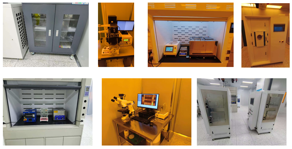

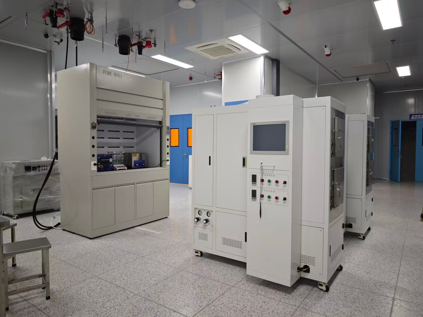
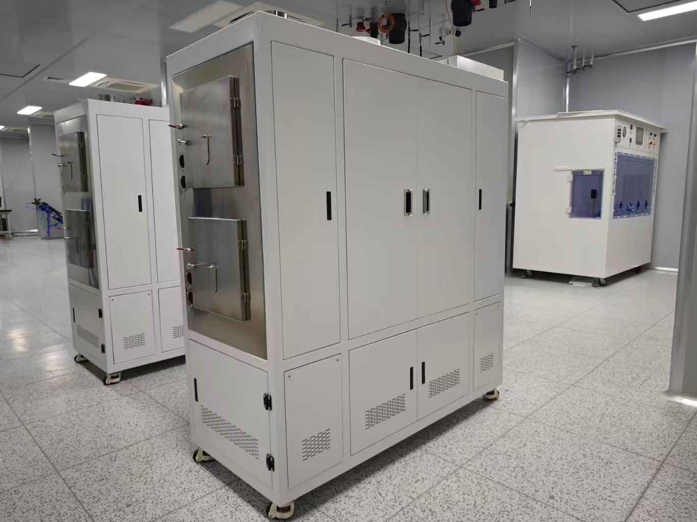

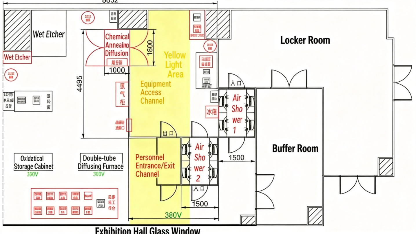
Targeting microelectronics, integrated circuits and other related majors in universities around the world, SUNY IC's teaching wafer manufacturing line focuses on the full process preparation of 1 μ m PMOS chips, integrating 10+independently developed core equipment, 120 ㎡ cleanroom renovation, and a complete set of teaching resources to create an integrated platform of "equipment process teaching research".
The modular design of the program can be divided into independent training or whole line linkage, suitable for undergraduate basic process training and graduate small-scale scientific research chip production needs, and supports interdisciplinary collaboration in circuit design, semiconductor materials, and other majors. Compared to industrial grade equipment, the cost of domestically produced consumables is more controllable, reducing operation and maintenance expenses by 30%. It can be delivered on a turnkey basis within 3-6 months without the need for multi-party coordination.
Equipped with full process security protection and intelligent monitoring system, in line with the management requirements of university laboratories; Supporting teaching materials, instructional videos, and other teaching resources, along with a 3-year warranty and lifelong technical support, help universities quickly establish production education integration training bases and cultivate composite semiconductor talents with both engineering thinking and practical abilities.
1. All-in-One Turnkey Solution: 10+ Core Equipment
2. Dual-Purpose for Teaching & Research: Undergraduate Training + Graduate Small-Batch Pilot
3. Cost-Effective: 30% Lower Operational Cost Than Industrial-Grade Equipment
4. Safe & Compliant: Meets Global University Laboratory Safety Standards
5. Quick Deployment: 3-6 Months From Order to Commissioning
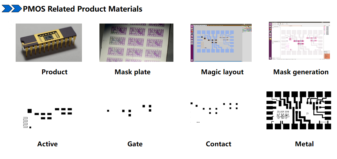
Designed exclusively for microelectronics and integrated circuit majors in universities worldwide, this turnkey wafer fabrication line is your one-stop solution to build a standardized training base. Centered on 1μm PMOS chip production, it covers all critical semiconductor processes—silicon wafer pretreatment, lithography, etching, diffusion, thin film deposition, testing, and more.
No more worrying about disconnected processes, expensive standalone equipment, or complicated infrastructure! We deliver a fully integrated system that balances technical precision and educational practicality, helping you bridge the gap between theoretical teaching and industrial practice in no time.
All equipment is tailored for university labs—user-friendly, safe, and stable:
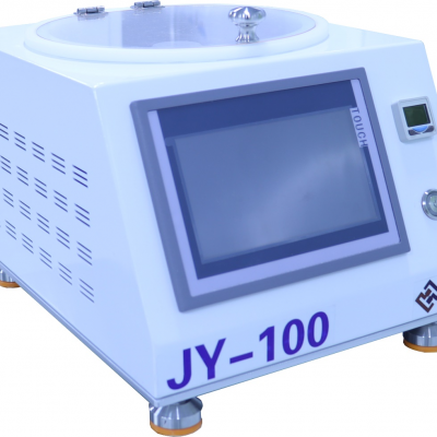
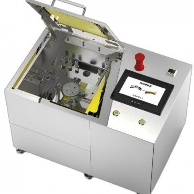
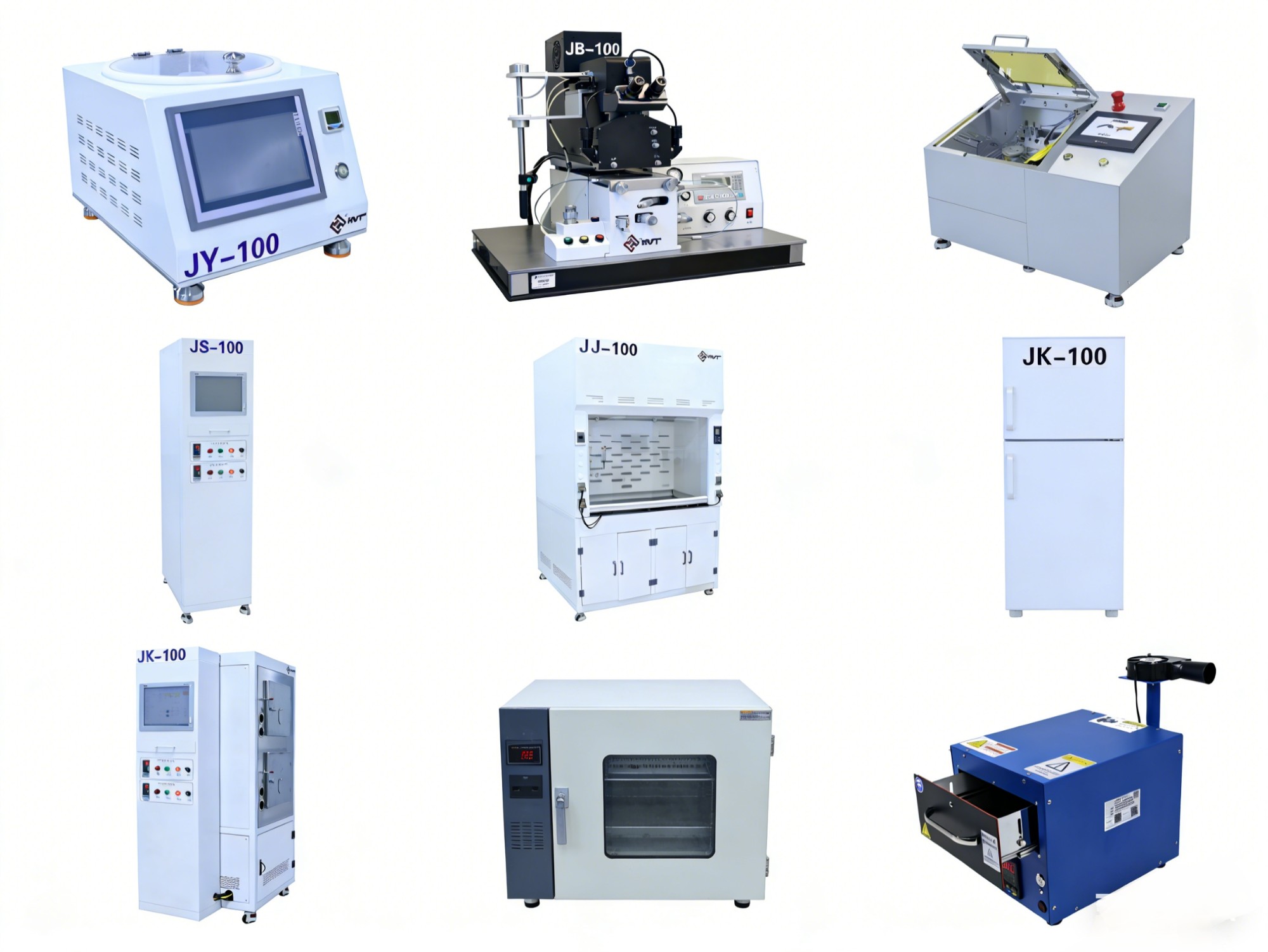
Spin Coater (JY-100): 100~10000rpm, 5~100mm wafer support, splash-proof design + fume hood
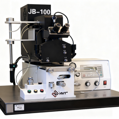
Lithography Machine (JB-100): ±1μm alignment accuracy, UVLED light source, binocular microscope
Wet Etching Machine (JS-100): 3 corrosion-resistant tanks, waste liquid recovery system
Double-Tube Diffusion Furnace (JK-100): 400-1260℃, ±1℃ constant temperature accuracy
Magnetron Sputtering Machine (JC-100): 6.0×10⁻⁵Pa vacuum level, ≤±5% coating uniformity
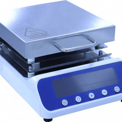
Plus: Optical Cement Drying Table, Photoresist Developer, Adhesive Removal Cleaning Machine, Oxidation Annealing Furnace, etc.
Supporting Tools: Anti-static workbenches, nitrogen cabinets, chemical storage cabinets, emergency eye washers, maintenance toolkits
Consumables Package: 2-inch/4-inch wafers (50pcs each), photoresist, developer, etchant, doping sources, inorganic cleaners
Testing Equipment: Four-point probe square resistance meter, optical thickness gauge, metallographic microscope, curve tracer
Undergraduate Training: Modular design allows single-process practice (e.g., independent lithography) to match curriculum
Graduate Research: Supports 500 4-inch wafers/year small-batch production, ideal for scientific projects and competition incubation
Interdisciplinary Support: Serves integrated circuit design, semiconductor materials, and microelectronic engineering majors
Affordable Procurement: Priced for university budgets, no phased purchases needed
Low Operational Costs: Localized consumables (30% cost reduction) + remote fault diagnosis
3-Year Free Warranty: Industrial-grade core components, lifelong technical support
Full Safety Protection: Chemical classification storage, exhaust systems, emergency shower/eye wash stations
Intelligent Control: PLC + touch screen, real-time equipment monitoring, process visualization
Compliance: Meets global university laboratory safety regulations
Turnkey Delivery: 3-6 months from order to use (no third-party coordination)
Teaching Resources: L-EDIT software, textbooks, operation videos, editable training guides
Customization: Adjust equipment/configuration based on your lab space and needs
| Item | Specification |
|---|---|
| Target Process | 1μm PMOS full process |
| Wafer Size | 5~100mm (2-inch/4-inch primary) |
| Lithography Accuracy | ±1μm alignment, 1μm exposure resolution |
| Furnace Temperature Range | 400-1260℃ (±1℃ accuracy) |
| Vacuum Level | 6.0×10⁻⁵Pa (magnetron sputtering) |
| Clean Room Grade | Class 1000 (yellow light area), Class 10000 (work area) |
| Annual Capacity | 500 4-inch wafers |
Ready to build your university's IC training base? Contact our team for a customized quote and free technical consultation!
Email: info@sunyinstrument.com
Tel: 0086-731-52373830
Mobile: 0086-17261398503
We provide global shipping and teacher training—your trusted partner for semiconductor education!